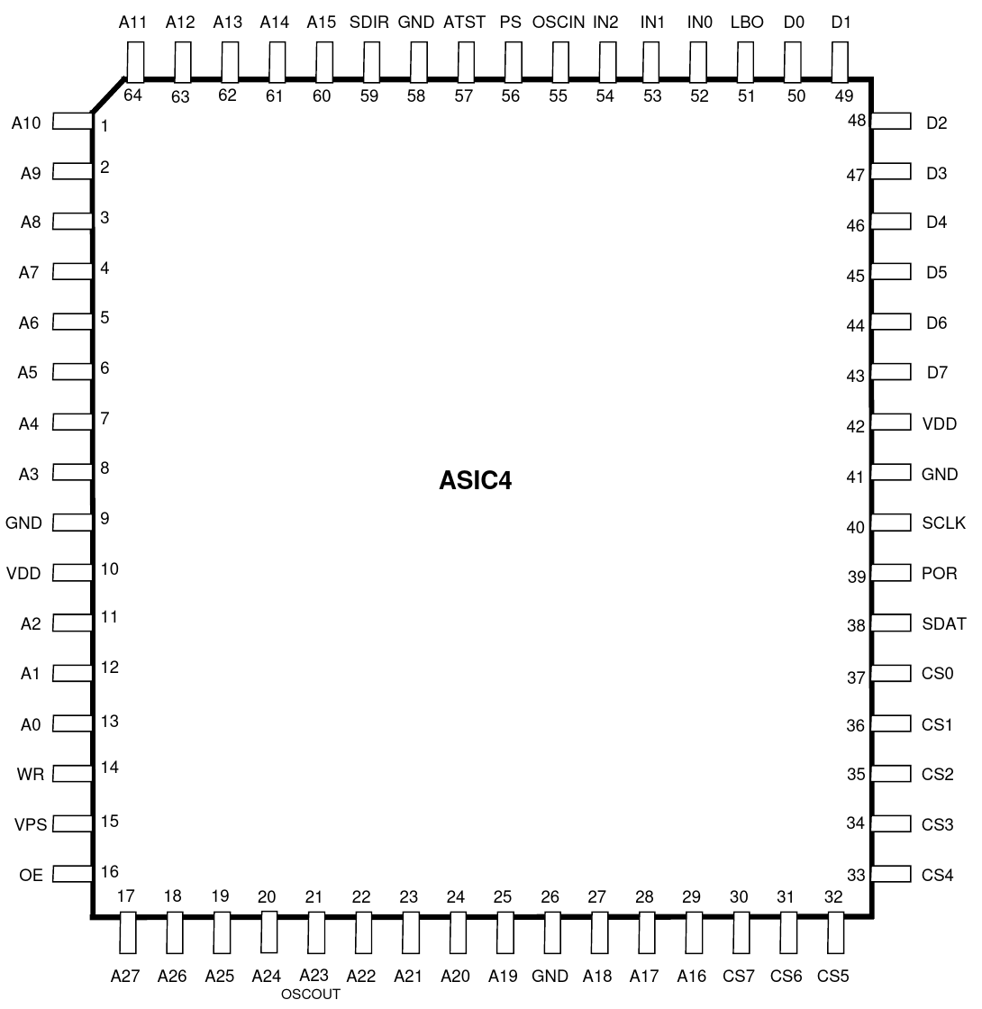
ASIC4 Extended Mode Addressing
Who wants a deep-dive into a tiny aspect of Psion SSDs and their ASICs?
I was using a PsiDrive a couple of months ago to dump a 2MB SSD. However, when I tried to extract the files, my FEFS extraction tool (siboimg) segfaulted halfway through. So, as I was in a rush, I decided to come back to it another day. Yesterday was that day.
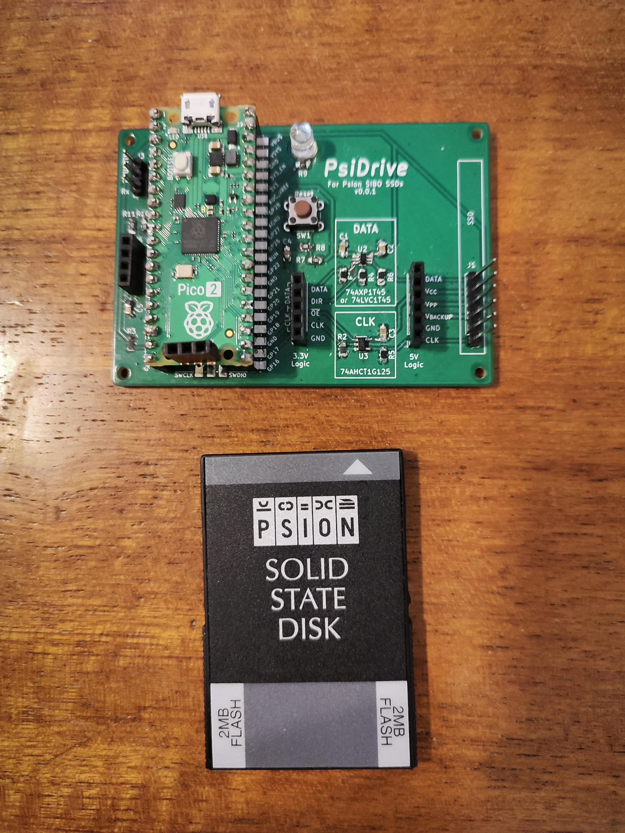
My first thought was that it could be a problem with the Pico 2, either with the code or the RP2350 A2 stepping chip. So, a couple of days before, I built a second PsiDrive and put in a Pico 1. But the fault remained with with Pico 1.
This meant it was an issue with my code somewhere. I thought it was strange that I’d never noticed it before, so it must be some weird edge case.
Psion SSDs are basically made up of a single ASIC and between one and eight storage chips. These chips could be ROM, battery-backed DRAM, battery-backed PS-RAM, or two different types of flash.
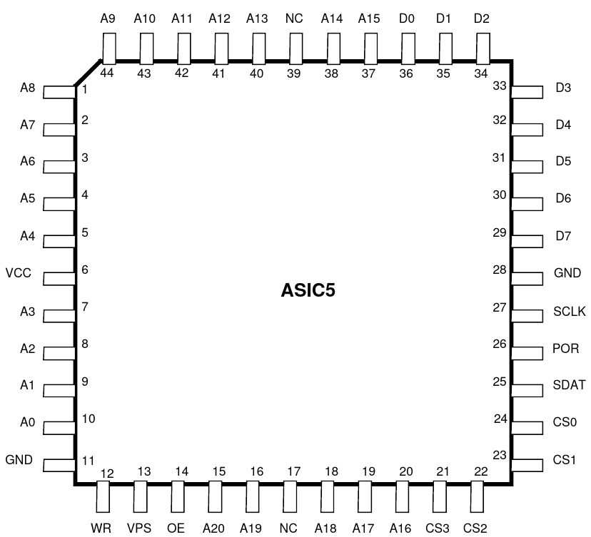
Psion used two different custom ASICs for their SSDs. The earliest ones use ASIC5, the later ones ASIC4.
Why 5 then 4? From what I gather, ASIC4 and ASIC5 were planned at roughly the same time, but ASIC4 went through a few changes before production, so was delayed. ASIC4 was originally meant to be a cut-down ASIC5 with just the storage parts remaining - things like the RS232 interface were removed. However, as time went on, ASIC4 had a few features added. It kept compatibility with ASIC5’s storage mode, but added some more ASIC4-specific modes for use with peripherals.
I actually have two Psion Games 2 SSDs - one with ASIC4 and one with ASIC5. This is great for testing. However, these ROM SSDs didn’t show up the edge case that cause this fault, as we shall see.
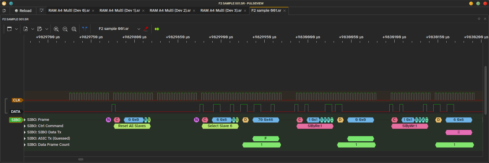
A quick side note: The Psion SIBO Serial Protocol (SIBO-SP) is a proprietary two-wire serial protocol, a bit like I2C with CLK and DATA lines, and the concept of master and slave devices. (From memory, the term “master” is never used in the HDK, but “slave” is.)
To talk to a slave, the master sends a control frame with an selection ID. For this discussion, all you need to know is ID:2 is ASIC5 and ID:6 is ASIC4.
So, the SIBO-SP control frame “Select ID:6” means, “Hello, are you an ASIC4?” If yes, the response will be a byte with information about how ASIC4 is set up. If no, the response will be 0x00.
(Side-side note: ID:2 is specifically ASIC5 in storage mode. ASIC5 also uses ID:3 for peripherals such as RS232 comms.)
ASIC4 and ASIC5 are configured using pull-up and pull-down resistors. These set the number of devices (memory chips), the size of each device (all the same), and a few things like a peripheral ID for certain commercial products (3Link).
ASIC5 can address up to 8MB in 4x 2MB banks. The #Psion SIBO Hardware Development Kit docs calls each chip a “device”, even though it refers to CS0-CS3 (chip select).
ASIC4 is a bit more complicated.
ASIC4 can work in three different modes:
- Pack (storage) mode: This is completely compatible with a normal ASIC5, so that it works with older SIBO devices like the MC range and the original Series 3. Accessed with ID:2, just like a normal ASIC5.
- Extended SSD mode: Can (or not? see the next post) address up to 4x 256MB memory devices. Accessed with ID:6, plus a pull-down on the Mode bit (M=0).
- Extended Mixed mode: Same as Extended SSD mode, but moves the storage to CS4-CS7 and also adds an extra 4 “peripheral” (IO) devices at CS0-CS4. Accessed with ID:6, plus a pull-up on the Mode bit (M=1).
The description of this in the Psion SIBO HDK is a little confusing. Maybe it’s just me, but I’ve read this paragraph regularly over the course of 8 years and it’s only today that I think I’ve got a grasp of what it actually means.
However, the HDK misses one vital piece of information.
When first talking to ASIC4, this is the process:
- Master “selects” slave ID:6 (“Hello, am I talking to ASIC4?”).
- Master requests a byte. if it’s ASIC4, it’ll get a non-zero response (“Yes, I am, and here’s how I’m set up.”) This includes the device (chip) size information (1 = 32K, 2 = 64K, etc).
- If ASIC4 sends a non-zero response, master reads a byte from ASIC4’s Register 1. ASIC4 sends an “extended info” byte with more information.
- Master then requests to send a byte to ASIC4’s Register 1, and sends back the device size info.
This last step always confused me. I can’t see it mentioned anywhere in the SDK, but it’s clear to see in my logic probe captures. If you don’t do this, you only see the first 32K of each device (device size of 0 also means 32K). I had no idea why this was needed, but I accepted it and added a comment to the code to come back to it later.
Chekhov’s byte.
Fast forward to yesterday.
I’d worked out that this fault wasn’t appearing when I used ASIC5 mode on an ASIC4. I’d also worked out that only the first chip was being selected. So, on a 2MB SSD with 2x 1MB chips, I was seeing the first 1MB twice.
So, my device/chip select logic was wrong.
I’d looked at the SDK, worked out that ASIC4 could address up to 256MB of data (A0-A27), and guessed that the device selection bits were at A28 and A29. And then I’d… not tested it properly? At least it seems that way.
But although that’s what seemed logical, that’s not what was happening.
That byte that gets sent back to ASIC4’s Register 1? That sets the addressing window on ASIC4. Which then sets the position of the device select bits.
The position of the bits can be moved!
So…
if _sizecode is 1 (32KB devices),   the device ID will be at:  14 + 1  = bits A15 - A17
if _sizecode is 3 (128KB devices),  the device ID will be at:  14 + 3  = bits A17 - A19
if _sizecode is 6 (1MB devices),    the device ID will be at:  14 + 6  = bits A20 - A22
if _sizecode is 7 (2MB devices),    the device ID will be at:  14 + 7  = bits A21 - A23
if _sizecode is 11 (32MB devices),  the device ID will be at:  14 + 11 = bits A25 - A27
if _sizecode is 13 (128MB devices), the device ID will be at:  14 + 13 = bits A27 - A29
So, if I send back 13 to ASIC4 Register 1, the device select bits will always be at A27-A31, no matter how big the SSD actually is. Likewise, if I send 1, it’ll truncate every chip to 32K.
Why haven’t I included _sizecode of 14 for 256MB? Because I couldn’t get it to work. It completely ignores those upper bits and only ever selects the first device/chip. I don’t know if there’s a secret way to get that working, but it’s not documented. As no 256MB #Psion SSDs exist, I might not know for a very long time.
Yesterday, I assumed that ASIC4 Extended SSD mode only used 3 bytes for addressing + device select. But writing that list of ASIC4’s modes earlier and re-reading the HDK prompted me to check. After some testing, I found that it does indeed use 4-byte addressing + device select, but for some reason can’t use 256MB devices with the method I’ve outlined above.
So, there will be an update to the #PsiDrive firmware being uploaded very shortly, with added compatibility for a series of comparatively massive SSDs (for the 90s) that have never existed.
I guess the fact that device selection bits can be moved means that the software doesn’t actually have to care too much about devices. If the bits for selecting a chip are directly above the address space, then you can address them like it’s just one contiguous block of data.
I just wish the bloody HDK had mentioned it!
For those who are interested, here is that paragraph from the #Psion SIBO HDK.
Putting ASIC4 into SSD mode makes the chip compatible with all current versions of existing SSD software in production by Psion including all HC, series 3/3a and MC software. In this mode, ASIC4 mimics an ASIC5 in pack mode (see next chapter). This is because ASIC4 was originally designed to be a cut-down version of ASIC5 and so from the outset it was necessary to make previously existing ASIC5 software run on the new chip. The maximum address space in SSD mode is 21 address bits and 4 chip selects (which comes to 4 x 2Mb). In ASIC4 Extended mode, ASIC4 is capable of addressing up to 28 address bits (256Mb). In this mode, in addition to the Info Byte, a further 4 bits of information can be elicited from the state of the address lines A27-A24 during reset. Of these bits, the state of A27 (bit M) determines whether ASIC4 is going to be used as a standard SSD (M=0) or in a mixed mode (M=1) comprising of memory devices and peripherals. It is only the latter case which is of interest to the potential developer since this is the mode intended specifically for peripheral type expansion. In mixed mode ASIC4’s address space is split into two equal halves. The lower half of the addressing range is set aside for memory-mapped peripherals and can be used for any purpose. The upper portion of the address space is reserved for pure memory.